These sections will help you to understand the design concept of the
Microvitec 'CUB' Monitor. They give very detailed descriptions of each part
of the circuit. It is very important that you read these sections before
attempting any of the fault isolation and repair procedures.
The power supply is a variable frequency, self oscillating, switching
flyback convertor type, providing mains isolation and three stabilised
voltages, of 18V, 124V and 200V.
1. Control Circuit - Description
A. Operating Normally in Ready State
(1) TR2 turns on a step voltage whose amplitude depends on the instantaneous
value of rectified mains across T2 primary.
(2) Current in winding and TR2 collector increases in a linear fashion from
zero, in which time energy is stored as flux in the transformer.
(3) During this time D22, D23 and D24 are reverse biased and any load energy
is supplied by C27, C28, C31 and C26, from previous cycle.
(4) TR1 performs a control function, supplied from a reference winding on
transformer (nominal +30V).
(5) During 'ON' time of TR2, the emitter of TR1 is held at a constant with
regard to reference rail from D18.
(6) The base of TR1 is fed directly from the reference rail, via R3, VR4 and
R5, any voltage change on the reference arising from a change of voltage at
the main output will vary causing the constant current source, used to
charge C16, to vary in sympathy.
(7) C16 charges on the current available from R10. The voltage across C16
increases until it reaches the gate trigger voltage of TY1. Then TY1
conducts and 'crow bars' base drive to TR2.
(8) TR2 ceases conduction and its collector voltage becomes positive. The
dV/dT at TR2 collector, is limited by C17, R12 and D17. As this occurs D22,
D23, D24 and D21 become forward biased and stored energy within the
transformer is transferred into output capacitors, and their respective
loads.
(9) Eventually voltages on D6, D21, D22, D23 and D24 anodes, collapse. TY1
is forced off prior to this stage by negative anode voltage, allowing TR2 to
turn on. Full base drive is then sustained by R16.

TR2 BASE Fuse in

TR2 BASE START-UP Fuse out
(10) HT stabilisation
(a) HT stabilisation is achieved by controlling the duty cycle of the
switching transistor.
(b) Increasing load = increased duty cycle and peak collector current.
(c) Increasing mains supply = increased operating frequency.
(d) HT adjustment is made by VR4.
(e) Extra damping for C14, R6 and D7, are required to limit Vce of TR2. D15
and D16 provide negative off drive and base current tracking. L2 optimises
storage time of TR2 for minimum switching losses.
(11) Max available power is determined by measuring, peak collector current
of TR2, and is sensed by R15. If voltage across R15 exceeds voltage across
TY1 gate cathode, then TY1 conducts turning TR2 off.
NOTE: This sequence occurs during start-up, at low mains and under fault
conditions.
2. Start-Up Procedure
A. Current required at start-up is small compared with base drive current
under normal operating conditions.
B. When turn on of TR2 occurs in this manner (once every 20ms) the
oscillation becomes self sustaining. R8 continues to supply current, but is
swamped by forward base drive from R16.

TR2 COLLECTOR Fuse in
3. Over Voltage Protection
A. Controlled by a second feedback loop attached to TY1, consisting of:
(1) A zener diode which senses the reference rail voltage and HT voltage
proportionally.
(2) If this reference exceeds zener voltage. D20 conducts, fires TY1 and
terminates drive to TR2. During which time enough volts are developed across
TY2 gate-cathode to cause conduction, and latch on.
(3) Drive to TR2 is stopped until C23 is fully discharged (10ms).
(4) Power supply is off until the next mains start-up pulse.
4. Short Circuit Protection
A. Short circuit or over current on any output rail represents an increase
in stored energy required from T2, therefore an increase in collector
current through TR2, detected by R15. Thus TY1 is fired and TR2 turned off.
B. Now operating in 'Burst Mode', that is, the power supply is initiated
under normal start-up conditions, but only operates for a few switching
cycles when the over current protection comes into operation, terminating
drive to TR2.
INPUT: Connections are made at PL101 - red, green and blue video, sync
options 1, 2, 3 and TTL video normal/invert. All inputs are flashover
protected by resistors and diodes. R,G,B drives are split in two ways:
1. Test selectable links TL103, R,G,B.
2. To IC101
Select Position 1: The input stage is in the linear mode, the video is
buffered and level shifted by emitter output stages. These provide
temperature tracking with TR103, 104 and 105 resulting in a stable black
level.
NOTE: In the linear mode only brightness variations of the video information
are possible using VR314.
Select Position 2: TR103, 104 and 105 bases are driven by IC101. This option
is used when driving from TTL video sources offering primary/secondary
colour and black and white drives.
NOTE: In the TTL mode, signal to noise immunity of system is very good.
IC101 can be used with negative TTL level video drives (R,G,B), in order to
invert video information.
Video inversion is achieved by toggling video polarity select line at PL101
pin 2 or TL101:
TTL Mode: Contrast of video information is tracked by varying available
potential across open collector load resistors, R114, 115 and 116 which are
supplied by TR101 from +12V, the base being driven from the contrast control
slider VR111, R112, C101 form a low pass filter and ensure smooth operation
of contrast control.
CRT Beam Current: Information is fed to D117, 118, from a constant current
source derived from 124V main HT rail. As CRT beam current increases D117,
118 junctions become more negative thus; D117 conducts more heavily causing
voltage to TR106 base to decrease. R136, C105 filter the signal, the derived
voltage is emitter followed and supplies TR103, 104 and 105 emitters directly.
Hence increases in CRT beam current, above a preset limit achieve an
automatic reduction in picture brightness.
NOTE: CRT beam limiting is preset depending on monitor model.
Brightness of display in all modes is adjusted by. VR134 enabling parallel
adjustment of R,G,B and black levels within a ±20V range from nominal:
400uA - High and medium resolution
700uA - 14" standard resolution TTL/Linear
900uA - 20" standard resolution TTL/Linear
TR102: A fast switching transistor used to derive mixed blanking pulses for
flyback blanking of video information. The base is driven from a potential
divider/mixer network, from a line flyback pulse and a frame flyback pulse.
Line flyback is advanced in phase with C225, to allow for transistor
switching delays. D107, holds TR102 in a semi-saturation state.
TR102 COLLECTOR with 10 to 1 scope probe
IC101 is also used to provide the following sync options:
Composite negative sync: Fed in on PL101, pin 7, ensure TL102 in non-active
position, allowing pin 2 of IC101, to be pulled high whereupon IC101
performs a sync inversion and provides an attenuated positive sync waveform
for driving sync separators of IC201, via R201 and TL106.
Composite positive sync: Fed in on PL101, pin 7 with TL102 in its grounded
position. IC101, now provides an output in phase with input and of suitable
amplitude for driving IC201 directly via R201 and TL106.
Separate negative line and field syncs: Ensure TL102 in non-active position,
line syncs are fed in on PL101, pin 5. IC101, performs an exclusive OR
function, the output being an inverted composite sync waveform.
Separate positive line and field syncs: Fed in on PL101, pin 7 in its
grounded position. TL106, is switched over to inverse field option. IC101,
provides an attenuated and buffered line sync feed for IC201, via R201.
Positive field sync information is fed directly PL101, pin 3 "sync3" input
by, TL106(B) and R202.
1. Line Timebase
A. Line oscillator function is based on IC201, providing three outputs:
(1) Horizontal drive pulses for control of line output stage.
(2) Vertical sync pulses compatible with synchronisation of IC301 field
output IC.
(3) A sandcastle pulse providing burst gate and clamping information.
NOTE: This facility is only used with IC TDA3301, currently required by '1
volt 75 ohm' linear, PAL input monitors.
2. Sync Separator
- IC201 (TDA1180P), incorporates separate noise gated sync separators for
line/field syncs, which accepts positive going sync pulses (or negative
going composite video) on pins 8 and 9.
- Output pulses from the line sync separator are used in conjunction with a
sync gate to synchronise line oscillator in a phase locked loop circuit.
3. Line Oscillator - Phase Detectors
- The line oscillator is timed by a network of resistors and capacitors on
pins 14 and 15 of IC201, used to derive a pulse of suitable mark/space
ratio for driving line output stages.
- IC201 contains two basic control loops, each containing a phase detector.
(1) The first phase detector compares output of the line oscillator with the
incoming line sync pulse. Phase detector output on pin 13, is filtered and
fed to the voltage control input of the oscillator on pin 15.
(2) The second phase detector, compensates for delays introduced by the line
output stage and compares line flyback pulses at pin 6, with oscillator
output. Phase detector output consists of a bi-directional current source
used to charge/discharge C213 on pin 5. Voltage derived from C213 is used to
control a phase shifter, which regulates the phase of the output pulse on
pin 3. Pin 5 also provides a 'line shift' function, by offsetting voltage
developed across C213. charged from VR220, R221 and R222 allowing phase
shift of ±1uS, between line scan and video information.
(3) A 7uS gate pulse from the line oscillator, whose phase position is
centred around the horizontal sync pulse. The gated pulse is used to control
the arrival of sync pulses at the sync phase detector for a duration of 7uS,
allowing latching and de-latching of line oscillator. Obtained by a
coincidence detector which compares the phase gate pulse with that of
incoming syncs.
(4) When the two signals are not aligned, the coincidence detector is used
to switch PLL filter into a short time constant mode, giving a high input
impedance at pin 12, thus increasing sensitivity and loop gain of
oscillator. The phase locked loop now has a low noise immunity but has a
very wide capture range. When aligned coincidence detector activates the
time constant switch, causing low impedance on pin 12, achieving a lower
sensitivity and loop gain, but providing a high degree of noise immunity.
During the 'locked' condition the PLL operates with a long time constant.
NOTE: A short time constant mode, can be achieved manually by connecting the
output of the coincidence detector on pin 11, to ground. Allowing the
oscillator to follow rapid fluctuations in line period, which may occur on
some non-standard signals.
4. Line Driver Stage
- Horizontal drive pulses from pin 3 (IC201) are D.C. coupled to TR201
and used to control driver transformer (T201) providing the impedance
conversion necessary to provide 600mA forward base current, for saturation
of line output transistor (TR202). Ringing is damped by R225 and C214 at
TR201 turn off, thus limiting its Vce to a safe value. HT supply to the line
driver comes from main HT supply rail, prior to R231 and HT scan interlock
(PL201 pins 5/6) allowing its operation to be checked independently of the
line output stage.
IC201 PIN 3 with 10 to 1 scope probe
TR202 COLLECTOR with 100 to 1 scope probe
5. Vertical Sync Output
- Output of field sync separator is used to drive vertical sync output
stage on pin 10 (IC201).
- In addition, this pulse is used internally to inhibit the first phase
detector during the field sync period, thus preventing 'top flutter' as a
result of equalising pulses.
6. Sandcastle Pulse
- Sandcastle pulse is on pin 7 (IC201), used on models with linear
interface PCB assembly consisting of two sections.
(1) Upper portion, suitable for burst gate and clamping operations from the
horizontal oscillator, thus ensuring an accurate phase relationship with the
video information.
(2) Lower portion, derived from a line flyback 'slice' for line blanking.
A. Line Output
- L202, L203 and T202 primary, are tuned during the flyback period by C222.
This lasts for 11.8/11.1uS, on 14"/20" monitors.
- Line output transistor TR202, is driven directly from the secondary
winding of T201. 'ON' current is controlled by R227, turn off dissipation is
minimised by L204.
- Line linearity correction is provided by L203, which is damped by C217,
R230. 'S' correction is provided by C218.
- Field timebase +25V (IC301) is achieved by rectifying a negative going
flyback voltage from a secondary winding on line output transformer. A
fusible resistor provides CRT protection under possible fault conditions.
LINE SYNC with 10 to 1 scope probe
TR202 COLLECTOR with 100 to 1 scope probe
B. EHT Supply
- 23.5kV required for CRT is generated by a tripler module driven from a
7.5kV, overwind on T203. Inductance of the transformer (between primary and
overwind), is tuned to the 7th harmonic of the flyback frequency by tripler
input capacitance and self capacitance of the overwind.
- The 'breathing' performance of the display is further improved by
deriving a high focus potential from a resistive thick film/substrate
potential divider from the EHT. giving rise to a constant bleed current from
EHT, thus lowering output impedance of the EHT circuit.
- An extra input diode within the tripler has its anode connected to the
tube base ground and via a beam current sensing circuit to 0V. C223 and a
network of resistors provide a load for the diode and effectively damp out
ringing which may occur during scan. The resulting 1000V which occurs across
C223 is used to generate A1 potential across CRT.
C. HT Supply
- Derived from the main secondary winding of the switch mode power supply
via R231. R231 is chosen to optimise picture breathing performance and offer
protection to TR202, during CRT flashover.
The field timebase function is carried out by IC301. *** **** *********
is determined by VR307, R308 and C303, producing a 100uS output pulse at
pin 12. Field sawtooth is derived from potential across C305 and C306 as
they charge towards +25V supplying R304, R305, R306 and R301. When field
scan is completed the 100uS pulse discharges C305 and C306 ready for
charging cycle to be restarted.
1. Field Linearity
- Sawtooth output on pin1 of IC301 via R313 and VR312 field linearity
control.
IC301 PIN 1 with 10 to 1 scope probe
2. Field Flyback
- In order to achieve a short field flyback time, a supply voltage larger
than required during scan, must be applied to field deflection coils during
flyback period. Made possible by using a separate field flyback generator,
within IC301.
- Main HT supply for IC301 is supplied to pin 5 via D302. During flyback
the generator doubles the supply on pin 5. The potential on pin 3 is
switched from 0V during scan to +25V during flyback The change in voltage
occurs on pin 5 via C304 causing potential to double during flyback.
- D302 isolates pin 5 from +25V supply. When deflection coil field has
collapsed and potential across field scan coils has fallen below +25V pin 3
is switched back to 0V and scan cycle resumed.
- Synchronisation of IC301 is achieved by feeding a positive going field
sync pulse on pin 8 of IC301.
IC301 PIN 8 with 10 to 1 scope probe
3. HT Supply for IC301
- Derived from a scan rectified rail from the line output stage. C305,
C306 are fed via VR306 (height control) from scan rectified supply and 12V
rail. Proportions of current and associated time constants R303, C301 and
D301 are used to minimise "picture bounce" thus maintaining accurate
tracking of the field scan with line scan amplitude during CRT beam current
variations, therefore reducing picture "breathing" effects.
4. Field Output
- Sawtooth output on pin 1 is applied to output stage (within IC301) and
scan output is available from pin 4 to field deflection coils. Current
within coils is sampled by R323, then fed back via R317 to the virtual
earth input pin 10 of IC301.
- Gain of output amplifier is set by the ratio of R314 and R317. DC
operating point by R318 and R316.
IC301 PIN 4 with 10 to 1 scope probe
5. Picture Geometry
- CRT E-W pincushion distortion is corrected by modulation of line
deflection current in transductor (T202) actively driven by TR301. which is
then fed from the parabolic waveform at the top of the S correction
capacitor C311. AC gain from the amplifying driver is used to control amount
of correction applied to CRT.
TR301 COLLECTOR with 10 to 1 scope probe
1. CRT Tube Base Panel (Refer to
diagrams)
2. Circuit Description
- All CRT electrodes are protected by a resistor, capacitor and spark gap.
(1) Scark gaps on all electrodes (except focus) are formed by a 1-2kV ring
trap gap, positioned within CRT base socket assembly. High focus voltage has
a separate 10kV spark gap contained within tube base socket.
(2) CRT cathodes are stood off from video outputs by 220 ohm resistors, the
grid 100k and A1's 820k.
(3) Decoupling of grid and A1's is achieved by C910 and C911.
(4) Focus voltage is provided by a potential divider located within tripler
module, providing an adjustable voltage of 5-8KV.
(5) A1 voltage is adjusted by VR932, offering a range of 350-820 volts.
(6) CRT heaters may be disconnected by removing TL901, in order to make
video adjustments.
(7) CRT cathodes are directly driven from video output stages mounted on CRT
panel.
NOTE: The component values given in this section refer to a standard 14 inch
model. For equivalent values, refer to the parts listing.
3. Video Output Stages - Circuit Description and Operation
NOTE: Red, Green and Blue video outputs are identical: the following text
refers to the red output stage.
- TR902 forms a class 'A' amplifier, AC gain is derived from the ratio of
R935 to R902, VR903 and DC gain by a DC offset current from R905 and VR906.
- R904 forms video output load and TR902 represents a low impedance drive
source to CRT input capacitance during its conduction.
- During turn off of TR902. the source impedance of the load R904 is
considerably reduced by TR901, ensuring a good 'pull-up' performance.
- Video compensation is achieved by split capacitances, C902, C903 to help
maintain a constant amplifier response curve over the full range of VR903.
- The emitters of TR902, TR904 and TR906 are connected together with a DC
reference of approximately 7.5V, used to set video black level voltage.
- TR907 performs line and field blanking of video information.
(1) TR907 is driven by negative (going) mixed blanking pulses from TR102.
TR907 conducts providing a 7.5V black level reference.
(2) During line and field flyback TR907 is turned off, forcing video outputs
off.
(3) Beam current information is sensed on tube base panel resistively,
across line output ground to 0V line by R937, D117, D118 on main PCB.
GENERAL
The 'Triple Standard PAL Interface Assembly' accepts RS170 video signals
(0.7v p-p video +0.3v p-p mixed -Ve Sync into 75R) and is designed to
interface between the Series 3 main chassis PCB assembly and the host
system. In wire-frame chassis format, output connections from interface to
main chassis PCB are made via hard-wired flexible leads and multiway plug-in
connectors PL102 and PL103, located on the main chassis. (see the
circuit diagram)
On some models, an interface input wiring harness lead assembly is provided.
This is supplied with one end only of the harness terminated in a 17-way
connector, the opposite wire ends being unterminated. Circuit details for
this harness lead assembly are given in the circuit diagram and connections
shown in the diagram and 'Table of Options', below.
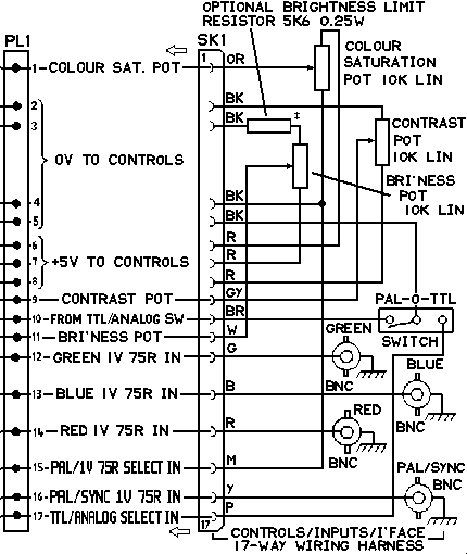
17-way connector
TABLE of OPTIONS
| Cnctr Pin No | Wire
Colour
| Available Standards
|
|---|
| TTL | 1V/75R | PAL
|
|---|
| 10 | Brown | O/C | 0V (S/C) | 0V (S/C)
| | 15 | Mauve | •
| > 0.7V < 12V (O/C) | 0V (S/C)
| | 17 | Pink | 0V (S/C)
| > 10.5V < 12V (O/C)
| > 10.5V < 12V (O/C) | |
NOTES:
- Not Critical (May be 0V to 12V or O/C)
0/C = Open Circuit (No connection)
S/C = Short Circuit (< 10 R) to 0V (Ground)
DOUBLE STANDARD/TRIPLE STANDARD INPUTS
Depending on how the interface assembly is installed, input modes for
either double or triple standards may be accommodated as follows:
- 1. TTL and PAL Video Mode - Double Standard
- 2. TTL, 1 volt 75 ohm and PAL Video Mode - Triple Standard
- Double Standard Input
When wired as indicated in the diagram - TTL' and 'PAL Video' Modes are
accommodated. Either one of these two modes may be selected by a 'single
pole change-over' switch as shown in the diagram.
- Triple Standard Input
Wiring details to accommodate Triple-Standard inputs and the various input
options are given in the '17-Way Harness Connections' Diagram and the
accompanying 'Table of Options'. Suitable additional switching may be
incorporated to accommodate the various options, depending on user
requirements.
OPERATIONAL NOTES
- PAL/Sync Input
When this input (PL1-pin 16) is used as the separate sync input of a 1v/75R
R.G.B. +sync video source, the amplitude of the sync MUST BE between 0.2v
p-p and 0.7v p-p, nominally 0.3v peak to peak. If the amplitude exceeds
these values, an 'In-Line' B.N.C. attenuator must be used.
- Sync-On Green Option
Setting Plug Link TL1' on the PAL Interface PCB to 'Position 2', allows a
'sync-on-green' 1V/75R RGB Video Source to be used.
NB: Note that the 'Green' 1V/75R video input (PL1-pin 12) now also becomes
the PAL input. See wiring diagram and 'Table of Options'.
Resistors employed in the construction are standard carbon film types of
¼W rating ±5% tolerance, except where indicated.
PARTS LIST
RESISTORS
| Circuit Reference | Component Reference | Description
|
|---|
| R5, 20, 21, 23, 25, 27, 28 | RF104DJO | 10K
| | R6, 8 | RF562DJO | 560R
| | R7, 30 | RF473DJO | 4K7
| | R9 | RF156DJO | 1M5
| | R10 | RF183DJO | 1K8
| | R11, 12 | RF392DJO | 390R
| | R13, 18 | RF225DJO | 220K
| | R14, 15 | RF123DJO | 1K2
| | R16 | RF272DJO | 270R
| | R17 | RF273DJO | 2K7
| | R19 | RF184DJO | 18K
| | R22, 24, 26 | RF103DJO | 1K0
| | R31 | RL101DJO | M/FUS, 10R
| | R32 | RF392DJO | 390R
| | R33 | RF152DJO | 150R
| | R40 | RF103DJO | 1KO
| | R101, 201 | RF104DJO | 10K
| | R102, 202 | RF222DJO | 220R
| | R103, 203 | RF100DJO | 1R0
| | VR1 | RQ102AL2 | POT PRESET 100R 0.1W H7
| CAPACITORS
| C1, 2 | CA337EN6 | ALUM/ELEC 33uF 16V
| | C3 | CK331JJO | ceramic/T 33pF 50V
| | C4 | CK121JKO | ceramic/T 12pF 50V
| | C5 | CK681JJO | ceramic/T 68pF 50V
| | C6, 8-15 | CK104FLO | ceramic/T 10nF 25V 20%
| | C7 | CM225KK6 | MET/T 0.22uF 100V
| | C16, 17, 18, 19, 20, 27 | CM105NL6 | MET/T 0.1uF 250V
| | C21 | CK222JKO | ceramic/T 220pF 50V
| | C22 | CM105NL6 | MET/P 0.1uF 250V
| | C23 | CK103JKO | ceramic/T 1nF 50V
| | C24 | CK151JKO | CER/T 15pF 50V axial
| | C25, 26 | CM4758K6 | MET/P 470nF 63V
| | C30 | CA107JL7 | A/ELEC 10uF 50V 20% RAD PR
| | C31 | CA105NL6 | ceramic/T 100nF
| | C101, 102, 201, 202 | CA2268M7 | A/ELEC 2.2uF 63V PREF
| | C103, 203 | CA107JL7 | A/ELEC 10uF 50V 20% RAD PR
| | C104, 204 | CM225KL6 | MET/P 0.22uF 100V
| | C105, 205 | CA109HM6 | ALUM/ELEC 1000uF 35V
| | C106, 206 | CM105NL6 | MET/P 0.1uF 250V
| | C107, 207 | CA478FM7 | ALUM/ELEC 470uF 25V
| DIODES
| D1, 2, 3 | DZ73560FRO | ZENER BZX79B5V6 2%
| | D4, 5 | DS4143UTO | 1N4148 THOMSON
| INTEGRATED CIRCUITS
| IC1 | IL3301UM3 | TDA3301 SELECTED
| | IC2 | IG4551UM2 | 4551
| | IC101, IC201 | IL19080S2 | TDA 1908
| CHOKES & DELAY LINES
| L1 | LW474SK2 | CHOKE 47uH
| | L2 | LW105SK2 | CHOKE 100uH
| | L3 | LW104SK2 | CHOKE 10uH
| | L4, 5 | LV001TA3 | CHOKE KAN K2819XM
| | L11 | LW154SK2 | CHOKE 15uH B78108-T1153-K
| | DL1 | ED0001P01 | DELAY LINE DL470
| | DL2 | ED0002P01 | DELAY LINE DL711
| CONNECTORS
| PL1 | KP0026A17 | PLUG 17-WAY 20/3457
| | PL2 | KP0026A16 | PLUG 16-WAY 20/3456
| | PL102 | KP0025A05 | PLUG 5-WAY 20/3445
| | PL103 | KP0025A03 | PLUG 3-WAY 20/3443
| | PL104 | KP0025A04 | PLUG 4-WAY 20/3444
| | TL1 | KP0024A03 | PLUG 3-WAY 20/3423
| MISCELLANEOUS
| FIT TL1 | KL9005Z02 | LINK TEST MOLEX 90059-0009 P/0
| | X1 | XC0014UU6 | CRYSTAL IQD TYPE 'P' A124D
| | 2 TRACK CUTS | BC0111I02 | PCB PAL INTERFACE
| | LK1, 2, 3 | WL2214TU1 | WIRE LINK 5mm x 14mm x 5mm
| | LK6 7, 8 | WL2212TU1 | WIRE LINK 5mm x 12mm x 5mm
| | LK9, 10 | WL2214TU1 | WIRE LINK 5mm x 14mm x 5mm
| | LK12, 13 | WL2212TU1 | WIRE LINK 5mm x 12mm x 5mm
| | A01647101 | I/FACE ASSEMBLY TPL/STD - MC REV 3 | | | | | | | |
BRIGHTNESS CONTROL LIMIT
If required - a resistor of 5K6 ohms 0.25W - may be incorporated in series
with the 'brightness' control to limit the control's range of 'brightness'
variation - as shown in the diagram.
AUDIO STAGE
On some versions of the interface, either single channel or twin channel
audio amplifier stages may be incorporated, depending on model and
specification.
Inputs and outputs for the audio stage(s) are marked as left-hand channel
(L) and right-hand channel (R) and are terminated in 2-pin connectors.
Normally, only a single channel audio stage is provided in most
applications.
Audio input to the stage may be fed across a 47k 'gain control' pot, with
the slider taken to the audio stages input.
TYPICAL AUDIO SPECIFICATIONS
Typical specifications for the audio amplifier stage are as follows:
| Input impedance: | 47 k nominal
| | Input sensitivity: | 100mV typical
|
| Output: | 2 watts max @ 1kHz into 16 ohms |
1. LUMINANCE CHANNEL (Y)
- The (-Y) signal contains:
(1) Video information
(2) line sync pulses
(3) frame sync pulse
- The incoming Y signal is attenuated by the potential divider, R16, R17
the resultant signal is then amplified by TR6.
- Transistors TR7, TR8 and TR9 have the following functions:-
(1) TR7 - Separates the sync pulses
(2) TR8 - Inverts the sync pulses
(3) TR9 - Buffers the sync pulses
R28 and R29 in the emitter of TR9, splits the voltage swing to produce a
'SYNC TTL' output.
- The rising edge of the sync output signal is used by C6, R30 and TR24 to
produce a pulse which has the same duration and timing as the colour burst
gating pulse on the +/- (R-Y) signal.
- The luminance signal on the collector of TR6, is clamped to the black
level by C10 and TR25.
- The black level is set by resistor/diode potential divider formed by VR1,
(R36, R37, R65 and 2 IN4148 diodes).
2. COLOUR DIFFERENCE CHANNELS
- The -(B-Y) Channel
(1) The -(B-Y) signal is attenuated by a potential divider network R32 and
R34. TR10 inverts and amplifies to produce + (B-Y). TR11 and C9 use the sync
pulses to clamp the + (B-Y) signal to the black level.
(2) TR21 merges + (B-Y) clamped signal to +Y clamped signal to produce the
BLUE output.
(3) TR22, is an electronic switch that has its threshold set by R56 and R57.
(4) The gain of TR22 is set by R58 and R59 to produce TTL levels. TR23
emitter follows the TTL signal which produces a buffered output.
- The +/- (R-Y) Channel
This channel is a phase alternating line (PAL) signal, which requires
alternate lines, inverted to produce + (R-Y).
(1) The incoming +/- (R-Y) signal is A.C. coupled by C17, C1 and TR1 thus
forming a unity gain, phase splitter.
(2) The non inverted output of TR1 drives an electronic switch (TR3). The
inverted output of TR1 is buffered by TR2.
(3) The (R-Y) switch is enabled during the colour burst, gating pulse.
(4) A set/re-set flip-flop switch formed by IC1C and IC1D works
in the following:-
(5) The outputs of 1C1D enable bi-directional switches which will either:
(a) Connect +(R-Y) through C1
(b) Connect inverted -(R-Y) through C2.
Thus producing +(R-Y). TR4 and TR5 clamp the +(R-Y) to the black level.
(6) The + (R-Y) clamped signal is added to the +Y clamped signal by TR13 to
produce +R signal.
(7) TR14 has its threshold set by R43 and R42. the gain is set by R44 and
R45, in order to produce TTL levels.
(8) TR15 emitter follows the TTL signal thus producing a buffered signal
output.
- THE (G-Y) OUTPUT
(1) This signal is generated by mixing the following:-
(a) The (B-Y) clamped signal. TR16 performs this mixing function
(b) The (R-Y) clamped signal, TR16 performs this mixing function
(2) The proportions of (B-Y) and (R-Y) clamped signals which are added
together are set by R54 and R40.
(3) G OUTPUTS
This signal is produced by the addition of the following signals:-
(i) (G-Y) clamped signal. TR17 performs this function.
(ii) +Y clamped signal, TR17 performs this signal function.
(4) TR18 has its threshold set by R48 and R49. the gam is thus set by R50
and R51 in order to produce suitable TTL levels.
(5) TR19 emitter follows the TTL signal and produces a buffered output.
GENERAL
- The 'Programmable-read-only-memory' (PROM) interface panel is used with
certain models in the 'SERIES-3' range of colour monitors. Two different
versions of the panel assembly may be used, depending on model and intended
country of operation:
- Interface connections:
(1) When installed, this panel assembly interfaces between input connector
PL101, located on 'SERIES-3' main chassis PCB and the monitor's 'user' 7-pin
Din input socket.
NOTE: The 'customer' contrast control VR111, shown on the
'SERIES-3' main chassis circuit diagram,
is not fitted as shown when the PROM interface is used. In this case, the
'customer' contrast control pot is connected to 'PL2', located on the PROM
interface panel.
(2) The 'PROM-INTERFACE CONNECTION DIAGRAM' provides wiring interconnection
details.
Note: This diagram appears to be missing.
CIRCUIT DIAGRAM
The circuit diagram for the 'PROM INTERFACE PANEL' provides circuit
details of the panel assembly.
Note: This diagram appears to be missing.
Only the ZX Spectrum Interface circuit diagram is provided.
LIST OF COMPONENTS
Details of possible circuit variations, used with different versions of
the panel, are shown in the accompanying Prom Interface Circuit Diagram.
Resistors employed in the construction are standard carbon film types of
¼W rating ±5% tolerance, except where indicated.
| Component Reference | Part No | Description
| RESISTORS
| R1 | RF683DJO | 6K8
| | R2 | RF391GJO | 39R 0.5W
| | R3,6,11,14,20,21,22,23,24,25,26 | RF222DJO | 220R
| | R4,7,10,12 | RF472DJO | 470R
| | R5,8,13 | RF103DJO | 1K0
| | R9,17 | RF102DJO | 100R
| | R15,18 | RF103DJO | 470R
| | R16 | RF683DJO | 1K0
| | R19 | | 2K2
| NOTE FOR APPLE MONITORS ONLY:
R9, R17 BECOMES 220R
| CAPACITORS
| C1 | CA2268M6 | ALUM/ELEC 2.2UF 63V
| | C2,3 | CM105ML6 | MET/P 0.1 UF 160V
| | C4,5,6 | CK151JKO | CER/T 15PF 50V
| DIODES, TRANSISTORS, INTEGRATED CIRCUITS
| TR1 | QS0337UTO | BC337-5
| | IC1 | IV7805LXO | 78L05
| | IC2 | IR18030AX2
| PROM TBP 18SA030N (PROGRAMMED INDIVIDUALLY FOR SPECIFIC MODEL)
| | D1,2-5 | DS4148UTO | IN4148 THOMPSON
| CONNECTORS
| PL1,3 | KP0026A10 | PLUG 10 PIN 20/3450 PRES
| | PL2 | KP0025A05 | PLUG 5 WAY 20/3445
| INDUCTORS
| L1,2,3 | LW104SK2 | CHOKE 10UH | | | | | |
CIRCUIT DESCRIPTION
- The purpose of the 'PROM' interface panel is to convert 4-Bit digital
video signals, normally referred to as 'R.G.B. & Intensity', into Linear
R.G.B. signals.
- Colour Combinations
(1) There are 16 possible colours which can be displayed (24
combinations).
(2) IC2, a fusible link PROM, provides sixteen 8-bit outputs corresponding
to one of the 16 addresses selected by the R.G.B. and intensity signals.
These outputs use 3-bits for RED and GREEN, and 2-bits for BLUE video,
hence; there are 8 levels of Red and Green and 4 levels of Blue available.
(3) Resistors R3 to R10 and resistors R11 to R18 form potential dividers
respectively between base and collector resistors of TR101, TR102, TR103,
located on the 'SERIES-3' main PCB. Resistors values are selected to
'weight' respective PROM outputs, to 'least significant' and 'most
significant' bits.
NOTE: When the 'PROM interface Panel' is installed, the moveable links
PL103, shown in the 'SERIES-3' main circuit diagram, should be fitted into
linked POSITION (1).
- +5 Volt Supply
IC1, C2 and C3 provide a regulated +5V supply for IC2.
- Protection & Termination
- Contrast Control
(1) Transfer TR1, R1 and an external pot connected to PL2 provide for
'customer' control of contrast on some models.
(2) TR1 forms an emitter follower, the voltage at the emitter determining
the video output amplitude on 'contrast'.
- Sync Signals
Sync signals are not required by the PROM circuitry and are passed
directly through the interface panel.
- R.F.I. Filtering
On models requiring R.F.I. filtering, L/C networks formed by L1/C4,
L2/C5 and L3/C6 are fitted on R, G & B outputs.