8-Bit Software
The BBC and Master Computer Public
Domain Library
Inside The BBC B
 [Back to Insides]
A home made BBC B
If you click on parts of this BBC B motherboard, you will be shown
information about what you have clicked on.
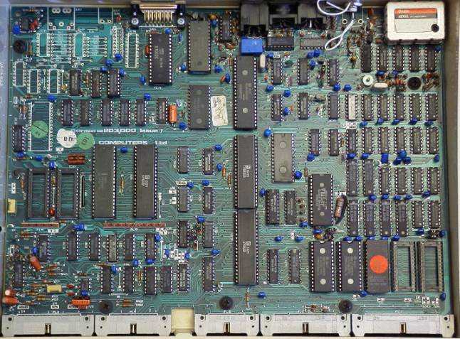 The above BBC B has no Econet but has a DFS interface fitted. The
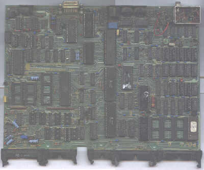
BBC B below has Econet and no DFS interface
The above BBC B has no Econet but has a DFS interface fitted. The
BBC B below has Econet and no DFS interface
BBC B Issue 7
IC1
6502A CPU
The microprocessor used in the BBC Micro is a 6502A running at either 1
or 2MHz. Most processing is done at 2MHz, including accesses to the
Random Access Memory (RAM) and Read Only Memory (ROM). The processor
slows down to 1MHz when addressing slow devices such as the 1MHz
Extension Bus, the Analogue to Digital Convertor (ADC), and the
Versatile Interface Adapters (VIA). A 16MHz crystal oscillator is used
to provide clock signals for the CPU in conjunction with divider
circuitry in the video processor ULA (IC6) which
produces 8, 4, 2 and 1 MHz signals. The 1MHz system clock is actually
generated by externally dividing the 2MHz signal by 2 using a D-flipflop
(half of IC34); the 1MHz signal out of the video ULA is only used for
driving ICs 5 and 15. Two more D-type flipflops (IC30) and an OR gate
are used to generate the 2MHz clock for the CPU, which has a specific
waveform requirement. Requests for a 1MHz processor cycle from the
address decoding are fed via an inverter (1/6th of IC33) to a D-flipflop
(half of IC31) which latches the request for a 1MHz cycle. At the
appropriate time, as governed by the 2MHz clock, one of the 2MHz clock
cycles is masked off by a D-flipflop (half of IC34). When this happens
the D-flipflop that latched the request is cleared, to reenable the 2MHz
CPU clock at the next appropriate clock phase.
IC2
6845 (CRT controller, CRTC)
This is the heart of the BBC Micro's video circuitry. Its major function
is that of displaying the video data in memory on a raster scan display
device such as a television or monitor. As a bonus, the sequential
nature of accessing the system RAM for the video display refreshes all
the DRAM storage.
The CRTC does not interfere with CPU access to the memory, as they
operate on alternate phases of the system clock.
The 6845 is responsible for producing the correct format on the display
device, positioning the cursor, and monitoring the light pen input.
Other video functions involving colour and Teletext are dealt with by
the video ULA (IC6) and the Teletext Character
Generator (IC5).
IC3
6522 (Versatile Interface Adapter, VIA)
A VIA has two sets of 8 I/O lines with two associated control lines,
known as Ports A and B. Each I/O line can be set to input or output
individually using the VIA's Data Direction registers; the control lines
(CA1/CA2, CB1/CB2) act as handshake signals for their respective ports.
The input and output registers are latched. The VIA also contains two
16-bit programmable timer/counters and a shift register.
The BBC Micro contains two VIAs. One (IC3) is dedicated to internal
system operation, the other (IC69) is available for
system expansion.
Port A of the system VIA acts as a slow data bus which connects to the
keyboard, the sound generator (IC18) and speech
system chips (IC98, IC99). Port B drives an
addressable latch which is used to provide read and write strobe signals
for the speech interface, the keyboard and the sound generator chip.
Also, coming from this latch (IC32) are control lines C0 and C1 which
indicate the amount of RAM devoted to the display memory to be 16K, 8K,
10K or 20K. Outputs 6 and 7 of the addressable latch drive the caps lock
and shift lock LEDs on the keyboard. Two I/O lines on Port B are used to
input the two 'fire button' signals from the paddle connector SK6 and
two more lines are used as response lines from the speech interface.
Each time the system VIA is written to, the latch connected to port B is
strobed by a flipflop which is triggered from the 1MHz clock signal.
Port A control line 1 (CA1) is used for detecting keyboard activity, CA2
is connected to the video vertical sync, to generate the Start of
Vertical Sync event. CB1 takes the ADC End Of
Conversion signal, and CB2 is used for the Light Pen Strobe signal.
IC4
6850 (Asynchronous Communication Interface Adapter, ACIA)
This device is used to buffer and serialise or deserialise the audio and
RS423 data. An Uncommited Logic Array (ULA) specifically designed for
the BBC Micro is also used in the serial interface (IC7).
Contained within this ULA is a programmable baud rate generator, a
cassette data/clock separator and switching to select either RS423 or
cassette operations. IC42 divides the main board 16MHz clock by 13 and
this signal is divided further within the serial interface ULA to
produce the 1200 Hz cassette signal. Automatic motor control of an audio
cassette recorder is achieved by a small relay
driven by a transistor from the serial interface ULA. The signal out of
the cassette is buffered and the incoming signal is suitably filtered
and shaped by a three stage amplifier, implemented using a LM324 quad
opamp (IC35).
Two forms of serial interface are provided. One is an audio cassette at
either 300 or 1200 baud and the other is RS423, over a whole range of
baud rates. (RS423 is electrically compatible with RS232C in most
applications.)
IC5
SAA5050 (Teletext Character Generator)
Display mode 7 is a Teletext character mode. When using this mode,
only 1K of RAM is devoted to the display memory and the characters are
held within it as ASCII bytes. To implement this an SAA5050 Teletext
character generator is used. IC15 latches the DRAM data going into the
SAA5050, which then translates these bytes into a standard
Teletext/Prestel format display.
A 6MHz clock signal is required for the operation of this device. This
signal is produced by knocking a reset flip flop (two quarters of IC40)
backwards and forwards from 8MHz and 4MHz clock signals. The resulting
flip flop output is then itself inverted according to the state of the
2MHz clock signal by an exclusive OR gate (.25 of IC38). Glitches on
this output are removed by R119 and C48 to produce the 6MHz clock signal
at IC37 pin 8.
IC6
5C094 (Video ULA)
The video processor device (IC6) is another custom ULA developed
especially for use in the BBC Micro. At the end of each CRTC 250nS
access period, it latches the byte from the RAM and, according to the
display mode in operation, serialises the byte into 1 bit stream of 8
bits or 2 bit streams of 4 bits etc. In this way, display modes varying
in width from 640 pixels in 2 colours to 160 pixels in 8 colours, which
may or may not be flashing, can be produced. Also, in the video
processor is a high speed piece of static RAM called a palette. This
memory can be programmed to define the relationship between the logical
colour produced by the RAM and the physical colour which will appear on
the display. Thus, in a 640 pixel mode, the two colours to appear on the
display need not be black and white, they may be, say, red and blue.
Note that the data in RAM is unchanged by the palette, it is the mapping
onto physical colours which changes.
Modes 0 through 6 in the Micro are so-called bitmapped screens, which
allow for raster graphics. With these screens, each pixel on the screen
corresponds directly with one, two or four bits in the video memory.
This method of producing video screens is expensive in memory, involving
a minimum of 8 kilobytes for the display.
IC7
2C199 (Serial ULA)
See IC4
IC8, IC9, IC10, IC11, IC12, IC13
81LS95
Six octal buffers, type 81LS95 (ICs 8-13) are used to switch control
of the RAM address lines between the Microprocessor and the CRTC.
IC14
74LS245 (TTL Octal transceiver)
Enables and buffers the RAM data lines to the system data bus. Is
disabled when the RAM is accessed by the CRTC.
IC15
74LS273 (TTL Octal latch)
See IC5
IC16
LM555 CN
A 555 timer circuit (IC16) provides a reset signal at power up or
when the reset key is pressed. Also on the circuit board is a power up
reset CR circuit from the +5 volt power supply (C10, R20 and D1). This
provides a signal called Reset A which is fed to the system VIA (IC3).
Whilst the 555 timer produces a general reset both at power up and when
the reset key is pressed, the CR signal Reset A only goes low at power
up. By interrogating IC3 on the occurrence of a general reset, the
system can thus detect whether this is a cold start, i.e. power up, or a
hot start, i.e. the BREAK key or reset switch being pressed when the
system has already been in use.
IC17
LM324N (Quad OPAMP)
See IC18
IC18
76489 AN
IC18 is a four channel sound generator chip which may be programmed
to generate sounds of varying frequency and amplitude on each channel. A
quad opamp (IC17) performs mixing the sound generator and speech
generator (IC98, IC99) signals and an auxiliary
audio signal from the 1MHz extension bus, amplifies and filters the
result, and feeds it to IC19.
IC19
LM386N-1
IC19 provides audio power amplification to drive a speaker (connected to
PL15).
IC20
74LS139 (TTL dual 2-to-4 decoder/latch)
Used in address decoding for the OS and language ROMs.
See IC52
IC21
74LS00 (TTL Quad 2-input NAND gate)
See IC24
IC22, IC23
74LS30 (TTL 8-input NAND gate)
See IC24
IC24
74LS138 (TTL 3-to-8 decoder/latch)
Used in address decoding for the I/O devices.
All the I/O hardware is located within locations &FC00 to &FEFF. These
three 256-byte address ranges (pages) are commonly referred to as FRED,
JIM and SHEILA. FRED and JIM are concerned with external user hardware
connected to the 1MHz bus and can optionally be
disabled; SHEILA contains all of the system's internal hardware device
registers. This is decoded by IC22 and via ICs 20 and 25, the OS ROM (IC51) is then masked off over this range of addresses.
ICs 24 and 26 decode the individual devices in this range; IC23 detects
when a slow 1MHz device is being addressed, initiating the system clock
circuitry to do a slow clock cycle.
IC25
74LS20 (TTL Dual 4-input NAND gate)
IC26
74LS139 (TTL dual 2-to-4 decoder/latch)
Used in address decoding for the I/O devices. See IC24
IC27
7438 (TTL Quad 2-input NAND gate, open collector)
IC28
74LS51 (TTL Dual 3-input AND-OR-Invert gate)
See IC44
IC29
74LS32 (TTL Quad 2-input OR gate)
IC30, IC31
74LS74 (TTL Dual D-flipflop)
Part of the clock generation circuitry. See IC6
IC32
74LS259 (TTL 3-to-8 decoder/latch)
See IC3
IC33, IC37
74LS04 (TTL Hex inverter)
IC34
74LS74 (TTL Dual D-flipflop)
See IC6
IC35
LM324N (Quad OPAMP)
See IC4
IC36
74LS10 (TTL Triple 3-input NAND gate)
See IC39
IC38
74LS86 (TTL Quad 2-input EXOR gate)
See IC5
IC39
74LS283 (TTL 4-bit adder)
Used in conjunction with IC36 and the signals C0 and C1 out of
IC32 to map the CRTC address lines
to the correct DRAM starting address.
IC40
74S00 (TTL Quad 2-input NAND gate)
See IC5
IC41
74LS02 (TTL Quad NOR gate)
In order for the receiving television to interpret the colour
information, a reference colour burst has to be provided at the
beginning of each line. A short burst gate signal immediately after the
horizontal sync pulse for each line is produced at IC41 pin 4, and is
timed by C45 and R109. This burst gate allows through a standard colour
subcarrier signal which the television uses as its colour phase
reference for that line. The PAL colour signal may be added to the 1v
video connector by closing link LK39, which adds a 470 pF capacitor
between the emitter of Q9 and the base of Q7. Diodes D20, 21 and 22
adjust the luminance for the three separate colour signals to create a
composite signal with better readability of dark colours when displayed
on a domestic television set.
IC42
74LS163 (TTL Synchronous binary counter with preset)
See IC4
IC43
74S04 (TTL Hex inverter)
IC44
74LS74 (TTL Dual D-flipflop)
ICs 44 and 45 are the core of the DRAM address
multiplexing circuitry. The multiplexing Row Address Strobe (RAS) signal
is produced by a D-flipflop (half of IC44) connected to the 8 and 4MHz
clock signals. This RAS signal then drives all of the dynamic RAMs via
R106. Column Address Strobe (CAS) signals are generated by one half of
IC45. In Model A computers having only one bank (8 devices) of RAM only
CAS 1 is used. Model B systems with 32kB of RAM have the second bank of
RAMs selected by a 74LS51 (IC28) which controls the 74S139 (half of
IC45) generating the CAS signals. The other half of IC45 is used to
select between the processor and CRT address lines. The actual switching
of the address lines is done by enabling one of the 81LS95 buffers
IC8-IC13.
IC45
74S139 (TTL dual 2-to-4 decoder/latch)
See IC44
IC46
74S74 (TTL Dual D-flipflop)
IC47, IC48
74LS86 (TTL Quad EXOR gate)
Used for colour generation on composite video. See IC6
IC49, IC50
74LS00 (TTL Quad NAND gate)
Used for colour generation on composite video. See IC6
IC51
23128 (Operating System ROM)
32 kilobytes of Read Only Memory are catered for in the Micro
address map. The upper 16 kB (C000-FFFF hex) of this are occupied
by the operating system ROM (IC51), with three pages of 256 bytes each
not used by the system ROM but mapped for use by I/O devices instead
(see IC24).
IC52
23128 Basic ROM
Apart from the OS ROM, four other Read Only Memories (ICs 52, 88, 100
and 101) can be on the main circuit board. In the Model A, four 4kB
ROMs may be in these four sockets in order to fill the 16kB address
space (8000-BFFF hex). In this case, a 2-to-4 line decoder (half of
IC20) is used to select which of the four devices is being selected by
the address lines A12 and A13. 8kB or 16kB ROM devices can be
accomodated with appropriate link settings (links 20, 22, 30 and 32-38),
but the maximum usable ROM size can only be 16kB.
In the Model B, significantly more flexibility is offered, with a ROM
Select Latch (IC76) being used to 'bank switch' one of up to four ROMs
into the address range. This allows for different programming languages,
system software extensions such as a Disc Filing System, or application
software like a word processor to be installed, and be activated when
needed. Normally, IC52 will contain the resident BASIC interpreter, with
ICs 88, 100 and 101 available for additional ROMs. If these ROMs all
stand by themselves, switching is by straightforward use of IC76 in
conjunction with IC20 to control each of the ROM's Chip Select lines.
Applications or extensions with a size of 16kB, but fitted in a pair of
8kB ROM devices can be accomodated by driving IC20 off address line A13
together with just one output of the ROM Select Latch (IC76). Overall
address decoding for the ROMs is by IC21 which decodes memory addresses
&8000-&BFFF and &C000-&FFFF. Locations &0000-&7FFF (&0000-&3FFF for the
Model A) are assigned to the system DRAM. This is
decoded by feeding A15 into IC21 pin 4.
Note that in early versions of the BBC Micro, the operating system may
be contained within 4 EPROM's in IC positions 52, 88, 100 and 101 with
the BASIC interpreter being located in IC51. As the OS ROM still needs
to occupy the range &C000-&FFFF, the address ranges which are assigned
to IC51 and ICs 52, 88, 100 and 101 are swapped using the two links
comprising S21. This arrangement is abnormal and it was phased out.
Users wishing to expand their systems support ROMs will have to have
their original operating system EPROM's exchanged for an operating
system ROM which should then be put in the usual position, with the two
S21 link wires changed from North-South to East-West.
IC53-IC60, IC61-IC68
4816AP-3 (16k x1 DRAM)
Random Access Memory on the Micro is provided by either 8 or 16 dynamic
memory devices (DRAM) (ICs 53-68).
In order to reduce the external pin count and simplify the internal
architecture of DRAM devices, their address inputs are usually
multiplexed. The 16kbit devices used in the BBC Micro require 14 address
lines, but by virtue of this multiplexing only 7 pins are required.
Addressing is achieved by first offering the lower 7 bits of the address
which are then latched by the DRAM on a Row Address Strobe (RAS) signal,
after which the high 7 bits of the address are set up and latched by a
Column Address Strobe (CAS) signal. At this point the required address
is complete, and data can be read or written. This sounds like a
time-consuming process, but by running the address multiplexing at twice
the speed of the system clock the DRAM data stays in step with the rest
of the system.
In the Micro, the RAS and CAS signals are generated from the 8, 4 and 2
MHz clock signals by ICs 44 and 45.
Two devices may have control of the RAM address lines: the 6502 CPU
(IC1) and the 6845 CRTC (IC2). The
CRTC generates the raster scan signals for the video display, together
with the address for each memory mapped byte of information in the RAMs
which is required to refresh the display.
DRAM ICs 61-68, and expansion ICs 69-77 are required for the BBC Model A
to be upgraded to a Model B.
IC69
6522 (Versatile Interface Adapter, VIA)
IC69 is the second versatile interface adaptor present in the BBC Micro.
Port A is used to provide a centronics standard parallel printer
interface, with the octal buffer IC70 being used to buffer the data
lines. Port B is left uncommitted and is free for use by the user for
input or output purposes.
IC70
74LS244 (TTL Octal Buffer)
See IC69
IC71
74LS244 (TTL Octal Buffer)
Buffers address lines A0-A7 for the 1MHz extension bus
IC72
74LS245 (TTL Octal Transceiver)
Buffers the data lines for the 1MHz extension bus
IC73
uPD7002 (Analogue to Digital Converter, ADC)
A four channel ADC facility with 10-bit resolution is provided by IC73.
This device connects straight to the Micro's data bus and is a dual
slope convertor with its voltage reference being provided by the three
diodes, D6, D7 and D8.
IC74
88LS120 (RS423 receiver)
The RS423 data in and out signals and request to send and clear to
send signals are interfaced by ICs 74 and 75 which translate
between TTL and standard RS423/232 signal levels. Note that this
is one of the few sections of circuitry on the Micro which
requires an additional -5v supply to be present.
IC75
DS3691 (RS423 driver)
See IC74
IC76
74LS163 (TTL Synchronous binary counter with preset)
ROM Select latch. See IC52
IC77
74LS00 (TTL Quad 2-input NAND gate)
ICs 77 to 88 are required for the 8271 DFS expansion
IC78
8271 (Floppy Disc Controller, FDC)
IC78 is a floppy disc drive controller circuit which is used to
interface to one or two single or double sided 5.25 or 8 inch floppy
disc drives. Logic signals from the controller to the disc drive are
buffered by two open collector drivers IC79 and 80. The incoming signal
from the disc drive is first conditioned by monostable IC87 producing a
pulse train with each pulse of fixed width. These pulses are then fed to
the data separation circuits ICs 81 and 82. This is a digital
monostable. IC86 divides the 8MHz clock signal down to 31.25kHz. ICs
83, 84 and 85 are then used to detect index pulses coming in from the
drive which show that the drive is ready for a read or write operation.
IC79, IC80
7438 (TTL Quad 2-input NAND gate, open collector)
Required for the 8271 DFS expansion
IC81
74LS393 (TTL Dual 4-bit binary counter)
Required for the 8271 DFS expansion
IC82
74LS10 (TTL Triple 3-input NAND gate)
Required for the 8271 DFS expansion
IC83, IC84
CD4013B (CMOS Dual D-flipflop)
Required for the 8271 DFS expansion
IC85
CD4020B (CMOS 14-stage binary counter)
Required for the 8271 DFS expansion
IC86
74LS393 (TTL Dual 4-bit binary counter)
Required for the 8271 DFS expansion
IC87
74LS123 (TTL Dual retriggerable monostable multivibrator, MMV)
Required for the 8271 DFS expansion
IC88
Empty ROM socket, occupied by a DFS ROM when DFS expansion fitted.
See IC52 for full information
IC89
68B54 (Advanced Data Link Controller Circuit, ADLC)
ICs 89 to 96 are concerned with the Econet interface.
IC89 is an Advanced Data Link Controller Circuit, type 68B54 which
handles the synchronous high-speed serial data transmission that is the
basis of the Econet protocol. Data to be transmitted on to the network
is fed from the ADLC to the line driver circuit, IC93, which is enabled
from the RTS line on IC89. Transmit data then goes through the line
driver circuit which produces a differential signal drive to the Econet
cables. Received data is detected and converted to a logic signal by one
half of IC94, a LM319 dual comparator. The received data is then fed
back to the data link controller circuit.
An Econet installation
has a single master clock station which provides the clock for the whole
of the network. This clock signal is transmitted around the network as a
second differential line signal and is used to clock the data in and out
of the data link controller circuits. The network clock is also detected
using one half of a LM319 comparator circuit, and the detector clock is
then fed to both receive clock and transmit clock inputs on the 68B54.
In the presence of a network clock, the monostable circuit, IC87, is
permanently triggered providing a data carrier detect signal for the
ADLC. Once the network clock is removed, the monostable immediately
drops out and the data carrier is no longer detected.
Econet is a broadcast network system on which a number of stations may
attempt to transmit their data over the network at any given time. In
this setup, a situation called a collision can occur when two or more
stations transmit at the same time. The transmitting stations should
detect the collision and back off before attempting to repeat the
transmission. Collision arbitration software is included in the Econet
system. Collisions on the network data lines result in the differential
signal on the two data wires being reduced. This condition is detected
by IC95 which is another dual comparator circuit. When there is a good
differential data signal on the network, one of the outputs of IC95 will
be low, in which case the output of IC91 pin 6 will be high, indicating
no collision. When there are no collisions on the network, and the
network clock is detected by the clock monostable, the data link
controller is clear to send data over the network. When there is a
collision on the network both outputs of IC95 will go high and the clear
to send condition will cease. Note that when the computer is not
connected to the network, a collision-like situation results, in which
case again the data link controller will not get a clear to send
condition. On receiving data, the data link controller circuit produces
interrupts which are tied to the central processor NMI line. These
interrupts are disabled by one half of the dual D-flipflop IC97. Once in
the data link controller interrupt service routine, IC97 is reset,
enabling further interrupts.
Each Econet system requires termination at the two extreme ends of the
network. Optional termination components were catered for on early Micro
circuit boards. These are: R26, R42, R53, R54, R56, C19, C22 and
D3. This has been changed to external termination later, which is more
flexible.
On early boards there also was a provision for a network clock source.
The 6MHz signal is divided by two to produce 3MHz and this drives IC90
which is a counter with decoded outputs. One decoded output of the
counter is selected to define the network clock frequency and the
counter then counts until this output goes high at which time the
counter resets and starts again. The selection of this clock signal
depends on the length of. the network with the longer networks requiring
a slower clock. Further selection divides the given frequency by two or
by four producing network clocks in the range 75 kHz to 625 kHz . The
other section of IC93 is then used to drive the differential clock
around the network, assuming that the computer is enabled to be a clock
source by select link 5.
Up to 253 (the numbers 0 and 255 being reserved, and the use of number 1
discouraged) stations may be connected to each Econet section with each
station being identified by a unique station identification number. This
station ID is programmed on the links into IC96, which can be read by
enabling the octal buffer.
IC90
Econet
See IC89
IC91
74LS132 (TTL Quad 2-input NAND gate, Schmitt-trigger)
See IC89
IC92
Econet
See IC89
IC93
75159 (Differential line driver)
See IC89
IC94, IC95
LM319 (Dual analog comparator)
See IC89
IC96
74LS244 (TTL Octal buffer)
See IC89
IC97
74LS74 (TTL dual D-flipflop)
IC98
TMS 6100 Speech Memory
See IC99
IC99
TMS 5220 Speech processor
The speech system device used is a TMS 5220 (IC99) which, on instructions
from the Micro, will produce at its output 'canned' speech from its
associated memory (IC98) or from speech data fed to it directly from
the Micro. The audio output of the speech system is filtered such that
it has a cutoff frequency of 7kHz.
IC100
Empty ROM socket, occupied by NET ROM when Econet expansion fitted.
See IC52 for full information
IC101
Empty ROM socket
See IC52 for full information
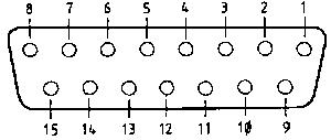
PL8
Disc Drive Port connector
34 pin IDC
PL9
Printer Port connector
26 pin IDC
PL10
User Port connector
20 pin IDC
PL11
1Mhz Bus connector
34 pin IDC
The address and data lines, A0-A7 and D0-D7, together with some page
select lines are available as the 1MHz extension bus to which various
peripheral devices may be connected, e.g. Teletext interface. All
accesses to this bus will be at 1MHz processor speed. The octal buffer
IC71 and the octal transceiver IC72, are used to interface these signals
to the internal data and address buses.
PL12
Tube connector
Selected address and data lines are available on the Tube connector
which is used to connect auxiliary processors into the system. This
should only be used by Acorn designed peripherals.
SK1
UHF TV modulator
UIM1233-E26 UHF MOD (ASTEC)
SK2
Composite Video Out BNC connector
SK3
RGB output connector
MAB6H 6 pin DIN
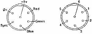
The red, green and blue logic signals produced by the video processor are buffered
by transistors Q4, 5 and 6 and fed out together with a composite sync signal
to the RGB connector (SK3). This output is suitable for feeding straight to
the gun drives of RGB monitors. The red, green and blue lines are summed together
by binary weighted resistors to feed Q7 which produces a 1V composite video
signal suitable for feeding to a monochrome monitor, on which the different
colours will appear as different intensities. By closing LK39 the chroma signal
present at Q9 will be added to this signal, enabling colour display on suitable
monitors.
The red, green and blue signals are summed with slightly different weight factors
to provide the input signal for the UHF modulator. The chroma
signal is always present here. The output of the UHF modulator is a TV signal
on channel 36, suitable for feeding to the aerial input of a domestic television.
This message came from Jamie: I just wanted to let you know about a possible
inaccuracy on http://www.8bs.com/inbbc.htm#SK3 . It says that the RGB signals
produced by the BBC are suitable for feeding straight to the gun drives of RGB
monitors. But as far as I know, this is incorrect - the RGB signals from the
BBC are TTL (a kind of primitive digital RGB) and need to be connected to the
TTL socket of a compatible monitor. This will pass the signal through a TTL
chip in order to convert the signals to normal analogue RGB. The BBC's RGB signals
will produce a picture on a non-TTL monitor, but they will overload it and could
damage the monitor's tube & chassis. Thanks and best wishes, Jamie.
I would appreciate it, if you can confirm this, you could let me know
SK4
RS423 connector
MAB5WH 5 pin DIN
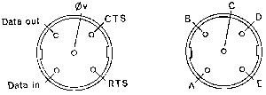
SK5
Cassette connector
MAB7SH-L 7 pin DIN
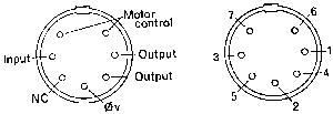
SK6
Analogue connector
15-pin female D type
|
1 - +5V |
9 - light pen strobe in |
|
2 - GND |
10 - fire button 1 |
|
3 - GND |
11 - Vref |
|
4 - analogue in CH3 |
12 - analogue in CH2 |
|
5 - analogue GND |
13 - fire button 0 |
|
6 - GND |
14 - Vref |
|
7 - analogue in CH1 |
15 - analogue in CH0 |
|
|
8 - analogue GND |
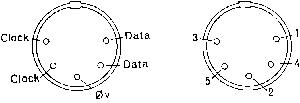
SK7
Econet connector
MAB5H 5 pin DIN
Relay
Miniature relay, normally open, used to control the cassette recorder
motor.
Colour frequency generator
See IC41
Keyboard
The keyboard circuit connects via PL13. A 1MHz clock signal is fed to a
74LS163 binary counter, the outputs of which are decoded by a 7445
decimal decoder driver circuit. These outputs sequentially drive each of
the ten rows of the keyboard matrix. If any key is depressed the 74LS30
gate will produce an output when that row is strobed, which will then
generate an interrupt to the computer on line CA2 of the system VIA
(IC3). On this interrupt, the system will enter the
key reading software. In order to discover which key was pressed, the
microprocessor will stop the 74LS163 counter, and load it directly with
the addresses of each key matrix row allowing it to interrogate each row
in turn. Also, the microprocessor loads the key column addresses into a
74LS251 data selector. The system will sequence through the row and column
addresses until it hits the key pressed, detected by line PA7 going low.
In this way, the microprocessor can interrogate each individual key in
turn until it discovers which one was depressed and causing the
interrupt. Once read, the keyboard regains its free running mode.
Power Supply
The power supply unit produces 5 volts at around 2 amps and -5 volts at
around 50 milliamps for use on the main circuit board. Some auxiliary power
for accessories may also be available on an external connector. The power
supply connects to the main circuit board by seven .110 fast on tabs with
the +5 volts being fed to three different points across the main circuit
board. These points are all connected together electrically. However, by
distributing the power in this way the need for very large copper tracks
to distribute power around the board is avoided. Most computers in production
will have a switch mode power supply, the circuit diagram for which is
given. It is not recommended that attempts should be made to repair this
power supply, instead it should be treated as a module to be exchanged.
A small number of early computers may have a linear power supply unit with
a conventional mains transformer and regulator circuit. These also should
be treated as modules to be exchanged rather than serviced.
[Back to Insides]